
張量處理單元
| 推出年份 | 2016年5月 |
|---|---|
| 設計公司 | |
| 體系結構類型 | 神經網絡 機器學習 |

張量處理單元(英文:Tensor Processing Unit,簡稱:TPU),也稱張量處理器,是 Google 開發的專用集成電路(ASIC),專門用於加速機器學習。[1]自 2015 年起,谷歌就已經開始在內部使用 TPU,並於 2018 年將 TPU 提供給第三方使用,既將部分 TPU 作為其雲基礎架構的一部分,也將部分小型版本的 TPU 用於銷售。
總覽[編輯]
2016 年 5 月,Google 在 Google I/O 上宣布了張量處理單元,並表示 TPU 已經在其數據中心內部使用了超過一年。[2][3]該芯片是專門為 Google 的 TensorFlow 框架(一個符號數學庫,用於機器學習應用程序,如神經網絡)設計的。[4]不過,截至 2017 年,Google 也將 CPU 和 GPU 用於其他類型的機器學習。[2]其他供應商也設計了自己的 AI 加速器,並針對嵌入式和機器人市場。
Google 的 TPU 是專有的,一些 TPU 的型號已經上市。在 2018 年 2 月 12 日,紐約時報報道稱 Google 將「允許其他公司通過其雲計算服務購買對這些芯片的訪問權」。[5]Google 曾稱,它們已用於 AlphaGo 與李世乭的人機圍棋對戰[3]以及 AlphaZero 系統中。Google還使用 TPU 進行 Google 街景中的文本處理,並且能夠在不到五天的時間內找到 Google 街景數據庫中的所有文本。在 Google 相冊中,單個 TPU 每天可以處理超過1億張照片。TPU 也被用在 Google 用來提供搜索結果的 RankBrain 中。[6]
與圖形處理單元(GPU)相比,TPU 被設計用於進行大量的低精度計算(如 8 位的低精度)[7],每焦耳功耗下的輸入/輸出操作更多,但缺少用於光柵化/紋理映射的硬件。[3]
根據 Norman Jouppi 的說法,TPU 可以安裝在散熱器組件中,從而可以安裝在數據中心機架上的硬盤驅動器插槽中。[2]
產品[編輯]
| TPUv1 | TPUv2 | TPUv3 | TPUv4 | Edge v1 | |
|---|---|---|---|---|---|
| 推出時間 | 2016年 | 2017年 | 2018年 | 2021年 | 2018年 |
| 製程 | 28 nm | 16 nm | 16 nm | 7 nm | |
| 裸晶尺寸/mm2 | 331 | < 625 | < 700 | < 400 | |
| 片上儲存/MiB | 28 | 32 | 32 | 144 | |
| 時鐘速度/MHz | 700 | 700 | 940 | 1050 | |
| 內存/GB | 8GB DDR3 | 16GB HBM | 32GB HBM | 8GB | |
| 熱設計功耗/W | 75 | 280 | 450 | 175 | 2 |
| TOPS | 23 | 45 | 90 | ? | 4 |
第一代 TPU[編輯]
第一代TPU是一個 8 位矩陣乘法的引擎,使用複雜指令集,並由主機通過 PCIe 3.0 總線驅動。它採用28 nm工藝製造,裸晶尺寸小於 331 mm2,時鐘速度為 700 MHz,熱設計功耗為 28–40 W。它有28 MiB 的片上存儲和 4 MiB 的 32位累加器,取 8 位乘法器的 256×256 脈動陣列的計算結果。[8]TPU 還封裝了 8 GiB 的雙通道 2133 MHz DDR3 SDRAM,帶寬達到 34 GB/s。[9]TPU 的指令向主機進行數據的收發,執行矩陣乘法和卷積運算,並應用激活函數。[8]
第二代 TPU[編輯]
第二代 TPU 於 2017 年 5 月發布。[10]Google 表示,第一代 TPU 的設計受到了內存帶寬的限制,因此在第二代設計中使用 16 GB 的高帶寬內存,可將帶寬提升到 600 GB/s,性能從而可達到 45 TFLOPS。[9]TPU 芯片隨後被排列成性能為 180 TFLOPS 的四芯片模塊[10],並將其中的 64 個這樣的模塊組裝成 256 芯片的 Pod,性能達到 11.5 PFLOPS。[10]值得注意的是,第一代 TPU 只能進行整數運算,但第二代 TPU 還可以進行浮點運算。這使得第二代 TPU 對於機器學習模型的訓練和推理都非常有用。谷歌表示,這些第二代TPU將可在 Google 計算引擎上使用,以用於 TensorFlow 應用程序中。[11]
第三代 TPU[編輯]
第三代 TPU 於 2018 年 5 月 8 日發布。[12]谷歌宣布第三代 TPU 的性能是第二代的兩倍,並將部署在芯片數量是上一代的四倍的 Pod 中。[13][14]與部署的第二代 TPU 相比,這使每個 Pod 的性能提高了 8 倍(每個 Pod 中最多裝有 1,024 個芯片)。
第四代 TPU[編輯]
第四代 TPU 於 2021 年 5 月 19 日發布。谷歌宣布第四代 TPU 的性能是第三代的2.7倍,並將部署在芯片數量是上一代的兩倍的 Pod 中。與部署的第三代 TPU 相比,這使每個 Pod 的性能提高了 5.4 倍(每個 Pod 中最多裝有 4,096 個芯片)。
參見[編輯]
參考文獻[編輯]
- ^ 云张量处理单元 (TPU) | Cloud TPU. Google Cloud. [2020-07-20]. (原始內容存檔於2021-06-13) (中文(中國大陸)).
- ^ 2.0 2.1 2.2 Google's Tensor Processing Unit explained: this is what the future of computing looks like. TechRadar. [2017-01-19]. (原始內容存檔於2022-02-26) (英語).
- ^ 3.0 3.1 3.2 Jouppi, Norm. Google supercharges machine learning tasks with TPU custom chip. Google Cloud Platform Blog. May 18, 2016 [2017-01-22]. (原始內容存檔於2016-05-18) (美國英語).
- ^ "TensorFlow: Open source machine learning" (頁面存檔備份,存於網際網路檔案館) "It is machine learning software being used for various kinds of perceptual and language understanding tasks" — Jeffrey Dean, minute 0:47 / 2:17 from Youtube clip
- ^ Google Makes Its Special A.I. Chips Available to Others. The New York Times. [2018-02-12]. (原始內容存檔於2022-04-08) (英語).
- ^ Google's Tensor Processing Unit could advance Moore's Law 7 years into the future. PCWorld. [2017-01-19]. (原始內容存檔於2019-02-18) (英語).
- ^ Armasu, Lucian. Google's Big Chip Unveil For Machine Learning: Tensor Processing Unit With 10x Better Efficiency (Updated). Tom's Hardware. 2016-05-19 [2016-06-26].
- ^ 8.0 8.1
Jouppi, Norman P.; Young, Cliff; Patil, Nishant; Patterson, David; Agrawal, Gaurav; Bajwa, Raminder; Bates, Sarah; Bhatia, Suresh; Boden, Nan; Borchers, Al; Boyle, Rick; Cantin, Pierre-luc; Chao, Clifford; Clark, Chris; Coriell, Jeremy; Daley, Mike; Dau, Matt; Dean, Jeffrey; Gelb, Ben; Ghaemmaghami, Tara Vazir; Gottipati, Rajendra; Gulland, William; Hagmann, Robert; Ho, C. Richard; Hogberg, Doug; Hu, John; Hundt, Robert; Hurt, Dan; Ibarz, Julian; Jaffey, Aaron; Jaworski, Alek; Kaplan, Alexander; Khaitan, Harshit; Koch, Andy; Kumar, Naveen; Lacy, Steve; Laudon, James; Law, James; Le, Diemthu; Leary, Chris; Liu, Zhuyuan; Lucke, Kyle; Lundin, Alan; MacKean, Gordon; Maggiore, Adriana; Mahony, Maire; Miller, Kieran; Nagarajan, Rahul; Narayanaswami, Ravi; Ni, Ray; Nix, Kathy; Norrie, Thomas; Omernick, Mark; Penukonda, Narayana; Phelps, Andy; Ross, Jonathan; Ross, Matt; Salek, Amir; Samadiani, Emad; Severn, Chris; Sizikov, Gregory; Snelham, Matthew; Souter, Jed; Steinberg, Dan; Swing, Andy; Tan, Mercedes; Thorson, Gregory; Tian, Bo; Toma, Horia; Tuttle, Erick; Vasudevan, Vijay; Walter, Richard; Wang, Walter; Wilcox, Eric; Yoon, Doe Hyun. In-Datacenter Performance Analysis of a Tensor Processing Unit™. Toronto, Canada. June 26, 2017. arXiv:1704.04760
 .
.
- ^ 9.0 9.1 Kennedy, Patrick. Case Study on the Google TPU and GDDR5 from Hot Chips 29. Serve The Home. 22 August 2017 [23 August 2017]. (原始內容存檔於2021-11-23).
- ^ 10.0 10.1 10.2 Bright, Peter. Google brings 45 teraflops tensor flow processors to its compute cloud. Ars Technica. 17 May 2017 [30 May 2017]. (原始內容存檔於2022-03-06).
- ^ Kennedy, Patrick. Google Cloud TPU Details Revealed. Serve The Home. 17 May 2017 [30 May 2017]. (原始內容存檔於2022-06-12).
- ^ Frumusanu, Andre. Google I/O Opening Keynote Live-Blog. 8 May 2018 [9 May 2018]. (原始內容存檔於2021-11-18).
- ^ Feldman, Michael. Google Offers Glimpse of Third-Generation TPU Processor. Top 500. 11 May 2018 [14 May 2018]. (原始內容存檔於2021-11-18).
- ^ Teich, Paul. Tearing Apart Google's TPU 3.0 AI Coprocessor. The Next Platform. 10 May 2018 [14 May 2018]. (原始內容存檔於2022-05-15).
外部連結[編輯]
- Cloud Tensor Processing Units (TPUs) (頁面存檔備份,存於網際網路檔案館) (Google Cloud 上的文檔)
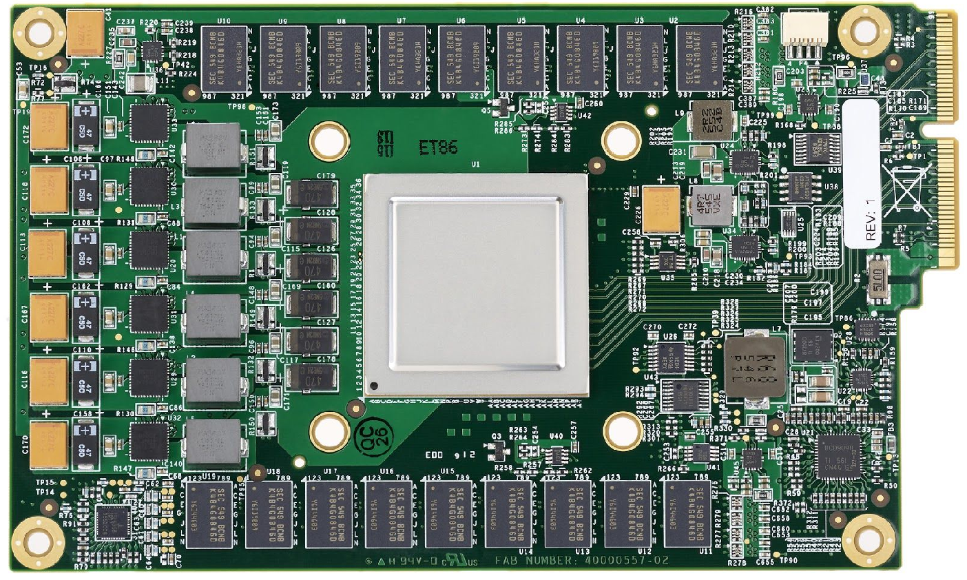
- Photo of Google's TPU chip and board (頁面存檔備份,存於網際網路檔案館)
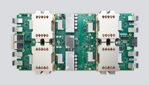
- Photo of Google's TPU v2 board (頁面存檔備份,存於網際網路檔案館)
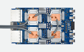
- Photo of Google's TPU v3 board (頁面存檔備份,存於網際網路檔案館)
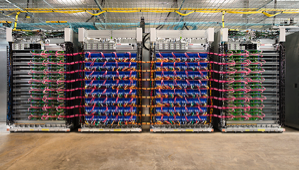
- Photo of Google's TPU v2 pod (頁面存檔備份,存於網際網路檔案館)
| ||||||||||||||||||||||||||||||||||||||||||||||||||||||||||||||||